
A MOSFET (Metal-Oxide-Semiconductor Field-Effect Transistor), also called a MOS FET, is a kind of field-effect transistor commonly made by oxidising silicon. The conductivity of the device is controlled by the voltage of the insulated gate, which enables it to amplify or switch electronic signals by adjusting the conductivity with applied voltage. The term MISFET is very similar to MOSFET, and IGFET is also a synonym for MOSFET.
The MOSFET transistor is the most widespread in digital circuits, and billions of them can be found in a single memory chip or microprocessor. Due to its ability to be made from either p-type or n-type semiconductors, pairs of MOSFETs can be combined to create switching circuits with extremely low power consumption, known as CMOS logic.
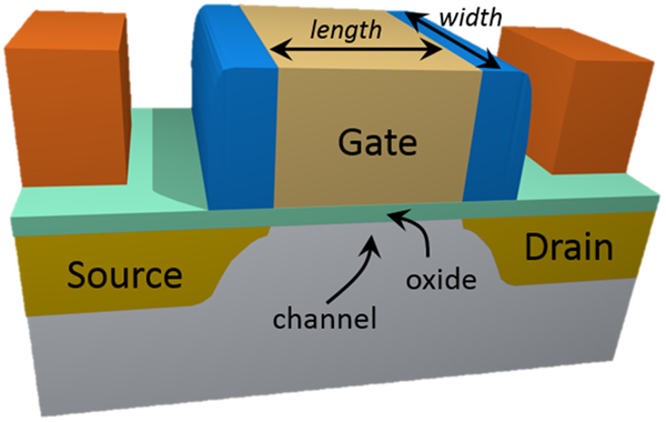
What Are the Components of Metal Oxide Silicon Field Effect Transistors?
Silicon is typically the preferred semiconductor material. However, some chip manufacturers have begun to use a silicon-germanium alloy in MOSFET channels. Despite the fact that some semiconductors, like gallium arsenide, have better electrical properties than silicon, they are not suitable for MOSFETs because they cannot form good semiconductor-to-insulator interfaces. Ongoing research aims to develop insulators with suitable electrical properties for use with alternative semiconductor materials.
To resolve the issue of elevated power consumption caused by gate current leakage, a large-κ dielectric material is applied as the gate insulator in place of silicon dioxide, and metal gates replace polysilicon. A thin insulating layer, traditionally made of silicon oxynitride or silicon dioxide, separates the gate from the channel. Some companies have begun incorporating a combination of high-κ dielectric and metal gates in the 45-nanometer node.
The application of the voltage between the gate and body terminals generates an electric field that penetrates through the oxide and creates an inversion layer or channel at the semiconductor-insulator interface. This inversion layer serves as a pathway for current to flow between the source and drain terminals. By adjusting the voltage between the gate and body, the conductivity of the inversion layer can be modulated, thereby controlling the flow of current between the drain and the source. This operation mode is known as the enhancement mode.
Evolution of MOSFET
In 1925, the concept of this type of transistor was initially patented by Julius Lilienfeld. Researchers at Bell Labs, including John Bardeen, William Shockley and Walter Houser Brattain, later proposed a structure similar to the MOS transistor during their investigation that resulted in the discovery of the transistor effect. However, the structure failed to produce the desired results due to the presence of surface state traps that immobilised electrons on the semiconductor surface. In 1955, L. Derick and Carl Frosch discovered a layer of silicon dioxide on a silicon wafer. A subsequent investigation uncovered that silicon dioxide was effective in stopping dopants from spreading into the silicon wafer. Building on this research, Mohamed M. Atalla demonstrated that silicon dioxide effectively solved the problem of a crucial class of surface states.
Building on Atalla’s research, in the 1960s, Atalla and Kahng successfully demonstrated a device that had the structure of a modern MOS transistor. The principles behind this device were similar to those attempted by Brattain, Bardeen and Shockley in their previous failed attempt to create a surface field-effect device. Although the device was initially perceived as inferior due to its 100 times slower performance compared to bipolar transistors of the time, Kahng highlighted several benefits, including ease of fabrication and its suitability for use in integrated circuits.
Functional Principle of MOSFET
The MOSFET operates by controlling the voltage and current flow between the source and drain terminals, acting as a switch. Its functionality is based on the MOS capacitor, which is a crucial component of the device. The type of the semiconductor surface between the source and drain terminals that is beneath the oxide layer can be transformed from p-type to n-type by applying a positive or negative gate voltage. For instance, a positive gate voltage generates a repulsive force which drives the holes located beneath the oxide layer down into the substrate.
The depletion region is populated by negatively charged bound charges linked to the acceptor atoms. As electrons are added, a channel is formed. A positive voltage also draws electrons from the n+ source and drains regions into the channel. If a voltage is applied between the drain and the source, the current can flow freely between the source and drain, and the gate voltage regulates the electrons in the channel. If a negative voltage is applied instead of a positive voltage, a hole channel will be created beneath the oxide layer.
Applications of MOSFET
Integrated MOSFET transistors are found in large quantities in digitally integrated circuits like microprocessors and memory devices. These transistors provide the basic switching functions needed for logic gates and data storage. MOSFETs are also utilised in a variety of applications where they may switch thousands of watts, such as variable-frequency drives, switch-mode power supplies and other power electronics functions.
MOSFETs are utilised in radio-frequency amplifiers up to the ultra-high frequency spectrum as analogue signals and power amplifiers, providing efficient power and energy utilisation. With an optimised powerfactor and energy efficiency, this type of transistor can be widely used in almost every data-transmitting device and is used in radio systems as oscillators and frequency mixers. In addition, MOSFETs play a role in audio-frequency power amplifiers for public address systems, sound reinforcement, and home and car audio systems.
Advantages and Disadvantages of Metal Oxide Silicon Field Effect Transistors
- It delivers improved performance even when operating at low voltage levels.
- The absence of gate current results in higher input impedance, leading to faster switching speeds for the device.
- These devices require minimal power and consume minimal current.
- However, when subjected to excessive voltage levels, it can cause instability in the device.
- Due to the thin oxide layer, these devices are susceptible to damage from electrostatic discharge.